1. Data format
The generally adopted, standard data format for PCBs is GERBER RS274X. In addition, to produce the boards, a file with the drilling, in EXCELLON or SIEB & MEYER format will be needed. All the files above are generated by programs dedicated for designing PCBs. We accept sets generated both in the metric and the inch systems.
2. Drilling
Drilling of the holes in printed boards is made on numerically controlled drills. These machines have drills with diameters ranging from 0.3 millimeter for 6.0 millimeter. Between these values, diameters every 0.05 millimeter are available. If necessary, we can also make holes with diameters larger than 6.0 millimeter by milling them.
The minimum via diameter in a 1.5 mm thick PCB is 0.3 mm. For thicker laminates, the minimum via diameter will be respectively bigger, so that the material thickness to the via diameter ratio is not higher than 5. For example for a 2 mm thick board the minimum via diameter will be 0.4 mm.
It is good to know that in order to make a via smaller than 0.5 mm, additional actions are required. This can affect the final price of the board. For this reason, provided that there is a sufficient space on the board, vias with 0.5 mm diameter should be used.
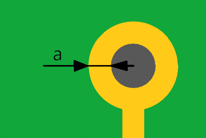
fig. 1
It should be remembered that the declared diameter of holes with plating is the target diameter. The manufacturer will also ensure that a drill with a respectively bigger diameter is used, to ensure that the hole has the preset diameter after the plating process.
An important parameter which should be remembered by the PCB designer is the minimum width of the copper ring around the hole [value "a" in figure no. 1]. The value "a" should not be smaller than 8 mils (0.2 mm) for vias and 10 mils (0.25 mm) for other plated through holes.
The assembly of certain elements requires holes to be made in the shape of slots. The minimum width of such a slot is 0.8 mm. It is best if such slots were declared in the drilling file or in the milling file.
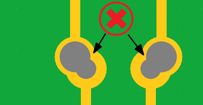
fig. 2
The holes that are to be made without plating should be placed in a separate file or clearly marked in the sent documentation. When no such information is given, all the holes not surrounded by copper will be made as non-plated-through.
Please make sure that, within the design, there are no overlapping holes. Any attempt to make a drilling program as presented in Figure no. 2 will result in damaging the drills. Such places must be corrected.
3. Copper layer
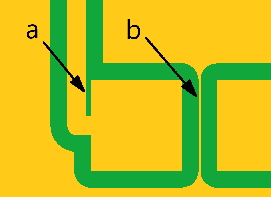
fig. 3
The minimum width of the path that we produce is 8 mils (0.2 mm). Likewise, the minimum distance between paths is also 8 mils (0.2 mm). These limitations also apply to cases seemingly not significant. Examples are presented in figure no. 3.

fig. 4
For double-sided boards with plating it is important that the designer takes care of a fairly even distribution of copper on the whole surface of the board. As a result, in the plating process, in every part of the board a layer of copper with similar thickness will deposit. An example of incorrect placement of copper is presented in figure no. 4.
4. Solder mask layer

fig. 5
For application of the solder mask we use two methods screen printing and photochemical. The screen printing method is less precise and can be used on simpler boards, namely on those on which there are no pads smaller than 20 mils (0.5 mm). We produce boards with solder mask in the following colors: white, green, blue, black and red.
To avoid applying the solder mask on pads, the size of the blank exposed in the solder mask should be slightly bigger than the size of the pad itself [value "a" in figure no. 5]. For screen printing technology the distance "a" should be at least 4 mils (0.15 mm) whereas for photochemical technology – 2 mils (0.075 mm).
Another limitation when applying the solder mask is the width of the "bridge" between pads [value "b" in figure no. 5] it should not be lower than 4 mils (0.1 mm).
5. Overlays layer

fig. 6
Overlays are applied to the printed board using the screen printing method. For the inscriptions and drawings forming the overlay on the printed board to be readable and aesthetic, the designer should follow the following constraints:
- the lowest width of the overlay line is 7 mils (0.18 mm) [value "a" figure no. 6]
- the lowest height of letters around 0.8 mm [value "b" figure no. 6]
- the minimum distance of the overlay lines from the pads 10 mils (0.25 mm) [value "c" figure no. 6]
A frequently made mistake, when designing the boards, is leaving the overlay on the pads. This does not interrupt manufacturing of the circuit, but can be a problem later, with the elements assembly.
Available overlay colors are white and black. Color black is practically used only on boards with white solder-mask. On other mask colors, white overlays look more impressively.
6. Mechanical treatment

fig. 7
Final mechanic treatment of the printed board can be performed with the use of milling or V-cutting. V-cutting is incising the boards at the top and bottom, so that the created panel can be broken up after installing elements [figure no. 7]. For dividing this panel an instrument called the separator is used. It is not recommended to manually break the boards.
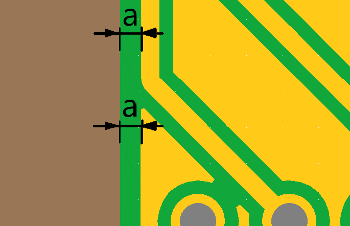
fig. 8
Milling is a slightly more expensive method than V-cutting. It must be applied wherever we are dealing with a non-rectangular shape of the board. For milling the dimensions we use cutters with a 1.6 mm diameter.
When designing a board it should be remembered that the minimum distance between copper and the edge of the board must be 20 mils (0.5 mm). This constraint applies both to paths and copper pours [figure no. 8].
7. Peelable mask

fig. 9
The peelable mask is used for protection of selected pads and holes from the effect of solder processes. These places can be, after removing the peelable mask, soldered again in the next process.
Such mask should be declared in a separate gerber file, with specified information whether it should be on the top or the bottom side. The designer should ensure that the area covered by the peelable mask is at least 1 mm bigger than the covered pad [value "a" in figure 9].
The maximum diameter of holes that we are able to cover with the peelable mask is 2 mm.
 Address:


 Phone:
 e-mail: